Structure description
P+/N junction on the 100x100 µm domain. Junction depth is 0.05 µm (50 nm). The junction extends laterally up to 50 µm.
The laser beam illuminates the wafer at position (0,0) with a Gaussian radius of 1 µm (the symmetry is cylindrial).
The mesh was automatically refined based on doping, laser generation and solution (electron, hole and potential).
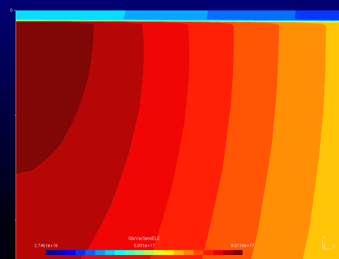
ELECTRON concentration (/cm^3) plot with gmsh.
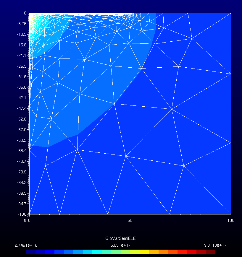
ELECTRON concentration (/cm^3) plot with gmsh. ZOOM around (0,0)
The P+/N junction is visible.
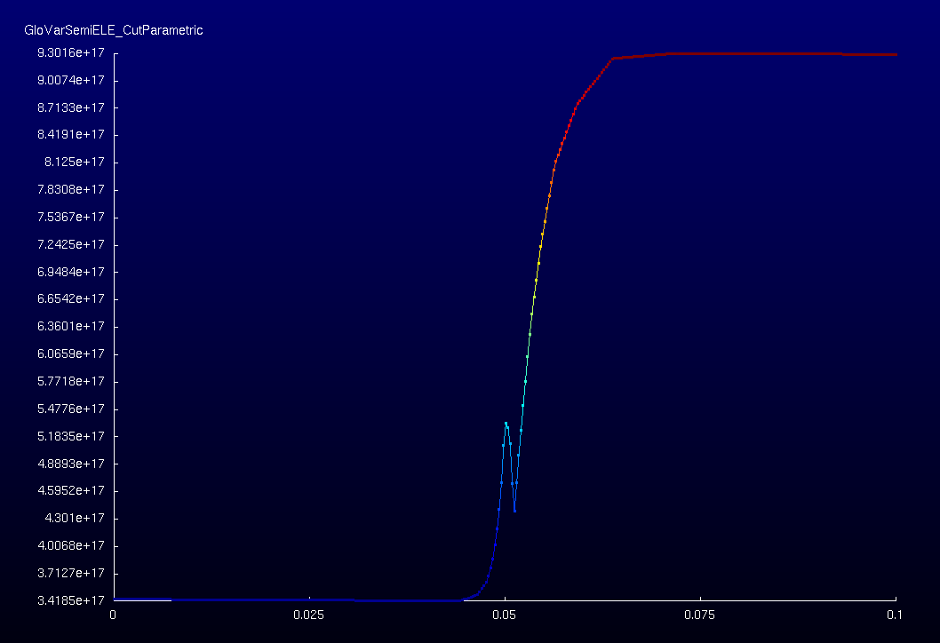
ELECTRON concentration cutline at x=0; y=u; with u=[0, -0.1 µm].
Due to the laser generation, the electron concentration is non negligible in the P+ part of the P+/N junction.
The sharp feature at the metalurgical junction (0.05 µm) is due to the band gap narrowing (BGN, Schenk's model).
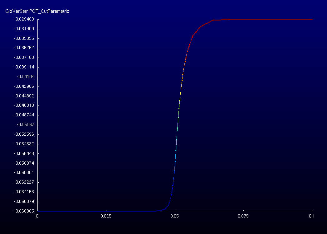
POTENTIAL cutline at x=0; y=u; with u=[0, -0.1 µm].
Due to the intense optical injection, the junction potential is trongly reduced (0.04 V)